
Nanofabrication
single photons at the chip scale requires state-of-the-art nano-fabrication techniques. The Quantum Photonics group has developed over the past years advanced processing methods for building nanostructures in gallium arsenide (GaAs) with tailored optical properties. These include passive devices such as waveguides, photonic crystals, and gratings, but also active electro-optic structures.

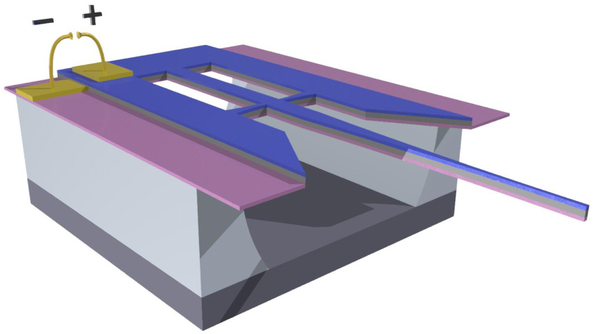
Our core strength, is the fabrication of suspended membranes with embedded self-assembled quantum emitters (quantum dots) [1].
We use a technique known as Inductively Coupled Plasma Reactive Ion Etching (ICP-RIE) to transfer computer-generated designs of nanophotonic devices, directly into the GaAs chip. We have also recently extended this process to include electrical control to the quantum dots, using doped layers in the membrane [2].
The fabrication of a chip involves several bulk and surface micromachining steps, to be carried out in a cleanroom environment. We have built a top infrastructure at the Niels Bohr Institute for GaAs processing, to perform nano-lithography, wet/dry etching, metal evaporation, atomic-layer deposition, and critical point drying. The entire processing of nanophotonic circuits can therefore be made in-house.
The group has also access to the Danish research infrastructure QUANTECH which features a 125 keV electron-beam lithography tool (Elionx F125) capable of writing patterns with few-nm resolution and a state-of-the-art scanning electron microscope (JEOL 7800). Additionally, we own an Oxford Instruments Plasmalab 100 for ICP-RIE dedicated to GaAs processing and a Polyteknik Flextura Cluster for electron-beam evaporation of metal contacts.
The research activity on nanofabrication revolves around novel processes and methods for the fabrication of high-quality and reproducible nanophotonic devices. We are interested in building a scalable platform which integrates efficient and indistinguishable single-photon sources with photonic integrated circuits and electro-optical devices.
MSc projects on nanofabrication of novel photonic devices are possible, provided that the duration is at least 1 year or longer.
Staff involved in nanofabrication activities: Zhe Liu (Process engineer, Quantech), Tommaso Pregnolato (PhD), Ying Wang (PhD), Asli Ugurlu (PhD), Camille Papon (Research assistant).
For further information and details about possible projects, please contact Assistant Prof. Leonardo Midolo (midolo@nbi.ku.dk) or Prof. Peter Lodahl (lodahl@nbi.ku.dk).